Duy-Ky Nguyen
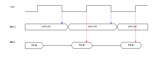
SPI has the following basic properties
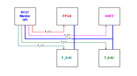
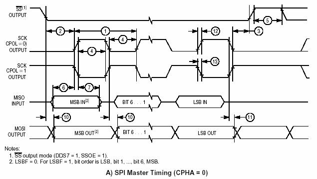
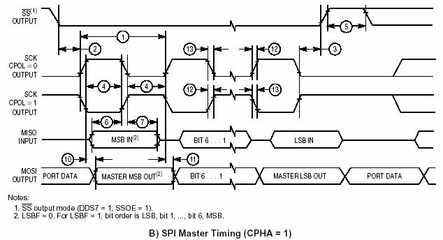
HC12 has master SPI interface with FPGA, DAC and UART. HC12 has 4 selectable SPI modes, but DAC and UART has only one that is CPOL=0, CPHA=0 in HC12. So FPGA will be implemented the same.
|
Num |
Function(1) |
Symbol |
Min |
Max |
Unit |
|
|
Operating frequency |
fOP |
DC |
1/2 |
E-clock frequency |
| 1 |
SCK period |
tSCK |
2 |
256 |
tcyc |
| 2 |
Enable lead time |
tLead |
1/2 |
- |
tsck |
| 3 |
Enable lag time |
tLAG |
1/2 |
- |
tsck |
| 4 |
Clock (SCK) high or low time |
tWSCK |
tcyc 30 |
128 tcyc |
ns |
| 5 |
Sequential transfer delay |
tTD |
1/2 |
- |
tsck |
| 6 |
Data setup time (inputs) |
tSU |
30 |
- |
ns |
| 7 |
Data hold time (inputs) |
tHI |
0 |
- |
ns |
| 8 |
Slave access time |
tA |
- |
1 |
tcyc |
| 9 |
Slave MISO disable time |
tDIS |
- |
1 |
tcyc |
| 10 |
Data valid (after SCK edge) |
tV |
- |
50 |
ns |
| 11 |
Data hold time (outputs) |
tHO |
0 |
- |
ns |
| 12 |
Rise Time |
|
|
|
|
|
|
Input |
tRI |
- |
tcyc 30 |
ns |
|
|
Output |
tRO |
- |
30 |
ns |
| 13 |
Fall Time |
|
|
|
|
|
|
Input |
tFI |
- |
tcyc 30 |
ns |
|
|
Output |
tFO |
- |
30 |
ns |
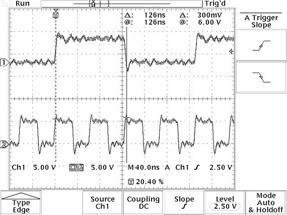
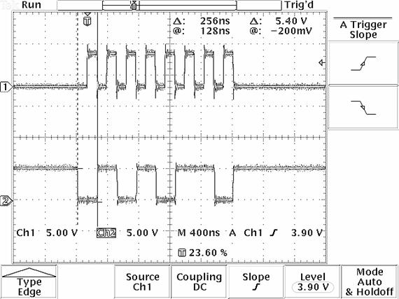
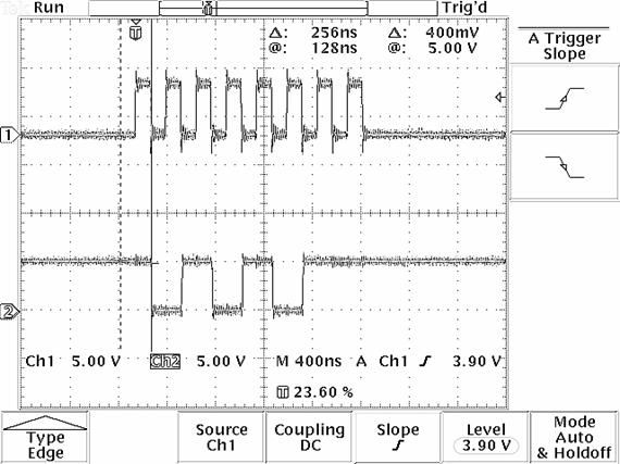
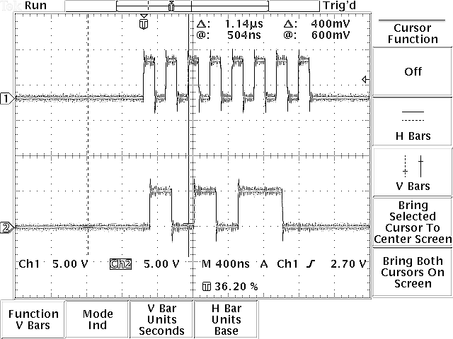
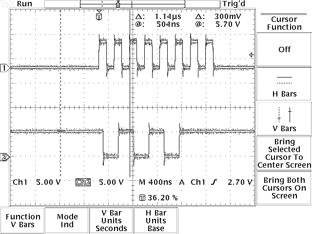
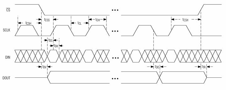
Below is expected SPI signals