
MicroController
Loi Ngoc Nguyen, Duy-Ky Nguyen, PhD
1. Introduction
The stimulus for the electronic computer was World War II. During the early part of the war, German submarines were wreaking havoc on British ships. Commands were sent from the German admirals in Berlin to the submarines by radio, which the British could, and did, intercept. The problem was that these messages were encrypted using a device called the ENIGMA, whose forerunner, incidentally, was designed by amateur inventor and former U.S. president, Thomas Jefferson.
Early in the war, British intelligence managed to acquire an ENIGMA machine from Polish Intelligence, which had stolen it from the Germans. However, to break a coded message, a huge amount of computation was needed, and it was needed very soon after the message was intercepted to be of any use. To decode these messages, the British government set up a top secret laboratory that built an electronic computer called the COLOSSUS. The famous British mathematician Alan Turing helped design this machine. The COLOSSUS was operational in 1943, but since the British government kept virtually every aspect of the project classified as a military secret for 30 years, the COLOSSUS line was basically a dead end.
The war also affected computing in the United States. The army needed range tables for aiming its heavy artillery and found calculating them by hand to be time consuming and prone to errors.
John Mauchley, an unknown professor of physics at the University of Pennsylvania, was aware that the army was interested in mechanical calculators. He knew of Atanasoff's work at IOWA Sate College to design a mechanical calculator using binary arithmetic and having capacitors for memory, which were periodically refreshed to keep the charge from leaking out. Modern DRAM chips work exactly the same way. Like many computer scientists after him, he put together a grant proposal asking the army for funding to build an electronic computer. The proposal was accepted in 1943, and Mauchley and his graduate student, J. Eckert, proceeded to build an electronic computer from 1943 to 1946, which they called the ENIAC (Electronic Numerical Integrator And Computer). It consisted of 18,000 vacuum tubes and 1500 relays. The ENIAC weighed 30 tons and consumed 140 kilowatts of power. Architecturally, the machine had 28 registers, each capable of holding a 10-digit decimal number. It was programmed by setting up 6000 multiposition switches and connecting a multitude of sockets with a veritable forest of jumper cables. Since the British kept all the aspects of the COLOSSUS in top secret for quite a long time, the ENIAC is seen as the world's first electronic digital computer.
John Von Neumann, one of the people involved in the ENIAC project, went to Princeton's Institute of Advanced Studies to build his own machine, the IAS machine. Von Neumann was a genius in league as Leonardo Da Vinci. He spoke many languages, was an expert in the physical sciences and mathematics, and had total recall of everything he ever heard, saw, or read. He was able to quote from memory the verbatim text of books he had read years earlier. At the time he became interested in computers, he was already the most eminent mathematician in the world.
One of the things that was apparent to him was that programming computers with huge numbers of switches and cables was slow, tedious, and inflexible. He came to realize that program could be represented in digital form in the computer's memory, along with the data. He also saw that the clumsy serial decimal arithmetic used by the ENIAC, with each digit represented by 10 vacuum tubes (1 on and 9 off) could be replaced by using parallel binary arithmetic. His basic design is now known as Von Neumann machine or stored program computer, and is still the basis for nearly all digital computers, even now, half a century later.
1.1. Computer Architecture
Stored Program Computer consists of 5 blocks:
- CPU: Central Processor Unit is used to process data
- ALU : Arithmetic Logic Unit
- CU : Control Unit
- Memory is used to store program (composed of many instructions) and data (information being processed by CPU). All programs are called software, all physical blocks of a computer are called hardware
- Primary storage: a must for a computer, it is called memory
- ROM: Read Only Memory is used to store permanent program, unerasable (read only, unwritable) so it is called firmware
- RAM: Random Access Memory is used to store data and program, it is also known as Read Write Memory due to its Read and Write capability (erasable)
- Secondary storage: optional, hardisk (HD), floppy disk (FD), magnetic tape, cassette, CD ROM
- Primary storage: a must for a computer, it is called memory
- Input Device is use4d to input program or data to CPU from external world
- keyboard (normally 101 keys, they are printable characters and symbols)
- keypad (normally 16 keys, they are 10 digits (0 to 9) and 6 characters A, B, C, D, E and F. A..F can be used with 0..9 to have hexadecimal number or used as special commands.
- Output Device is used to display data or machine status interacting with user
- monitor (or Video Display Unit, VDU, similar to TV)
- LCD (Liquid Crystal Display similar to calculator or watch). Without LCD, it is not known if we have a correct key in, even worse we do not know the computed result, an error message (status) such as divide by 0
- Printer to obtain a hard copy for storage.
- Bus is used to transfer data or instruction among the blocks. For simplicity, all blocks are connected to a common bus. At an instant, CPU can interface with only 1 block of memory, input or output which are identified by their address. In addition, data to memory can be Read or Write. So there are 3 types of bus
- data bus is used to transfer information (data or instruction), 8-bit computer has 8 data lines (wires) as a data bus
- address bus is used to show which block to communicate(memory, input or output), the memory size determines the number of address lines . 8-bit computer does not mean 8 address lines;
- control bus needs to discriminate Read or Write, thus there are 2 lines for Rd and Wr
Input and output devices are also called peripheral devices.
1.2. Data Transfer
Direction of data transfer is very important in a computer, bidirectional is R/W (Read/Write), unidirectional is R or W only. Note that R or W is due to CPU.
- (R) reads data into CPU from a memory or an input device;
- (W) writes data (result) or status (error message) in CPU (registers) to memory or output device.
1.3. Number Systems
A r-radix (r-base) has r digits (0, 1, ..., r-1) to represent a number.
A 10-radix number is called decimal number, a 2-radix number is called binary number, a 16-radix number is called hexa-decimal number.
For example,
A decimal number has 10 digits: 0,1,2,3,4,5,6,7,8,9; for example
A binary number has 2 digit: 0 and 1, for example
a binary number is not only long but also difficult to read and write and prone to error. However, binary numbers are used in digital computers, so hexadecimal numbers are used instead due to direct conversion between them.
A hexadecimal number (hex number) has 16 digits, there are 10 digits available: 0 to 9 and 1 digit cannot have more than 1 symbol, so A (10), B (11), C (12), D (13), E (14), F (15) are used to represent the remaining 6 digits. The decimal number 685 above can be rewitten as
To convert between hex numbers and binary ones, 1 hex digit is equivalent to 4 bit
| Hexadecimal | Binary |
| 0 | 0 0 0 0 |
| 1 | 0 0 0 1 |
| 2 | 0 0 1 0 |
| 3 | 0 0 1 1 |
| 4 | 0 1 0 0 |
| 5 | 0 1 0 1 |
| 6 | 0 1 1 0 |
| 7 | 0 1 1 1 |
| 8 | 1 0 0 0 |
| 9 | 1 0 0 1 |
| A | 1 0 1 0 |
| B | 1 0 1 1 |
| C | 1 1 0 0 |
| D | 1 1 0 1 |
| E | 1 1 1 0 |
| F | 1 1 1 1 |
For example,
1.4. Internal Signals
In the real world, there only exist analog signals within some range, for example a voltage from 0 V to 10 V (continuously), temperature from 00 to 1000. But in computers, there only exist digital signals in some length (bits) to represent data or instructions. These digital signals are in the form of binary numbers composed of bits (binary digits 0 or 1). A 4-bit number is called a nibble, 8-bit number is a byte, 16-bit number is a word. All data and instructions are stored in internal registers (in CPU) or in locations of external memory (out of CPU). Internal registers are identified by their names, external locations in memory are identified by their addresses. In 8-bit computers, a storage unit is of 8 bits length for internal registers and external memory and recognized as below
0	1	0	1	1	0	0	1
MSB							LSB
In 16-bit computer, the length of storage units is 16 bits and they are partitioned into high byte and low byte
High Byte (Hi-Byte)   | Low Byte (Lo-Byte)
15 14 13 12 11 10 9 8 | 7 6	5 4 3 2 1 0
MSB                                       LSB
LSB stands for Least Significant Bit, and MSB for Most Significant Bit.
Thus 1 storage unit can hold different information: 00000000, 00000001, 00000010, ..., 11111100, 11111101, 11111111. Using hex numbers is very simple, recall that 4 bits are replaced by 1 hex, thus the range of 1 byte is or
By convention, binary numbers are followed by b, a hex numbers followed by h, decimal numbers have no postfix; for example
thus computers with larger storage unit can hold more informations in each storage unit.
In computers, all informations are stored as binary numbers which can represent printable and unprintable symbols. The printable symbols are characters (A..Z, a..z), integers (positive or negative: 2, -10, ...), real numbers (floating-point numbers: 2.73, -1.45, ...) and symbols (+, -, /, ., @, ..). They are all keys on a keyboard except functional keys (F1..F12). The unprintable symbols are the function keys and other internal symbols under CPU control such as EOL (End of Line), EOF (End of File), Enter, ... If we write software for our own uses, we can assign different content numbers to different symbols, recall that 1 byte can hold up to 256 different informations, ie. 256 different symbols. However it is necessary to have a convention for software to be used by others. The most popular one is ASCII (American Standard Code for Information Interchange) such as
0: 30h, 1: 31h, ..., 9:39h; A: 41h, B: 42h, ..., Z: 5Ah; a: 61h, b: 62h, ..., z: 7Ah
ASCII has 128 symbols which can be represented by 7 bits, thus 1 byte (8 bits) can be used for this purpose with 1 spare bit.
The followings are to represent a number.
1.4.1. Unsigned Integer
1 byte gives numbers , or , ie. 256 numbers.
1.4.2. Signed Integer
In 1 byte, MSG is reserved for sign, , thus the remaining 7 bits are for value. For positive integers, we have , ie. or . For negative integers, we have , there is neither nor , so or
1.4.3. Floating-Point Number
Floating-Point numbers represent a very larger or very small value using a few digits. This scientific notation is composed of a signed integer called mantissa (M) and a signed integer as exponential (E).
For example, number 65535 can be written in the following forms
Note that the decimal point can be at any position, hence the name floating point.
By convention, mantissa is a fraction number like 0.65535 above
As signed integers, both MSB's in mantissa and exponential are used to indicate sign. Consider a 1-byte floating-point number, we have
- 4 bits for both F and E, thus , hence the range is and or roughly , the resolution is .
- 5 bits for F and 3 bits for E, thus , hence the range is and , or roughly , the resolution is .
Thus, higher resolution results in lower range. This resolution causes errors called round-off errors.
To increase resolution and range, double precision has double number of bytes using in single precision. For example, integers have 1 or 2 bytes, floating-point numbers have 4 or 8 bytes.
2. Micro-Processor, Micro-Computer and Micro-Controller
In the transistor generation, a CPU is composed of many modules (PCB, Printed Circuit Board). Integrated technology allows dozen of transistor on a single chip, thus a CPU reduces to a single module. VLSI (Very Large Scale Integration) allows dozen thousand earlier and few million now transistors on a single chip, then a CPU shrinks to a single chip and it is called Micro-Processor (MCU, mP)
2.1. Micro-Processor and Micro-Computer
2.1.1. Intel Family
In 1969, Intel Corporation USA was founded to make memory chips. The year after 1969, Busicom Corporation required Intel to research and develop CPU on a single chip for calculators. Gordon Moore and Robert Noyce at Intel were responsible for the project of the first 4-bit i4004 MPU from 1969 to 1971. i4004 (prefix i for Intel) has the area of and the consumption of 150 mW compared to and 150kW of the ENIAC, although the computing capability of this MPU is many times higher than that of ENIAC. ENIAC has 19000 tubes including memory, i4004 has 2300 transistors without memory, and i86484 has 1.2 million transistors. Intel did not expect anybody other than the original customer to be interested in them, so they set up a low volume production line. They were wrong, there was a tremendous amount of interest, so they set about designing and made a general purpose 8-bit i8080 MPU in 1973. This product took the industry by storm, and instantly became a mass market item, Intel sold millions. In 1976, Intel came out with i8085, a repackaged i8080 with some extra input/output features. Then came the i8086, a true 16-bit MPU on a single chip. The 8086 was designed to be somewhat similar to the 8080, but it was not completely compatible with the 8080.. The 8086 was followed by the 8088, which had the same architecture as the 8086 (16-bit internal registers), and ran the same programs, but had an 8-bit bus instead of a 16-bit bus, making it both slower and cheaper than the 8086. When IBM chose the 8088 as the MPU for the original IBM PC in 1979, this chip quickly became the personal computer industry standard.
In subsequent years, Intel came our with the 80186 and 80188, essentially new versions of the 8086 and 8088 respectively, but containing a large amount of input/output circuitry as well. They were never widely used.
Neither the 8088 nor the 8086 could address more than 1 megabyte of memory. By early 1980s this became more and more of a serious problem, so Intel designed the 80286, an upward compatible version of the 8086. The basic instruction set was essentially the same as that of the 8086 and 8088, but the memory organization was quite different, and rather awkward, due to the requirement of compatibility with older chips. The 80286 was used in the IBM PC/AT and in the midrange PS/2 models. Like the 8088, it was a huge success.
The next logical step was a true 32-bit MPU, the 80386. Like the 80286, this one was more-or-less compatible with everything back to the 8088, which was a boon to people for whom running old software was important, but a nuisance to people who would have preferred a simple, clean, modern architecture unencumbered by the mistakes and technology in the past. Like the 80286, this chip is widely used. The 80386SX is a special version of the 80386 designed to fit into an 80286 socket to provide a partial upgrade for existing 80286 machines.
The 80486 is upward compatible with the 80386. All 80386 programs will run on the 80486 without modification. The primary difference between the 80486 and the 80386 is the presence of a floating-point coprocessor, memory controller, and 8K on-chip cache. In addition, the 80486 is typically 2 to 4 times faster than the 80386, and is better suited for multiprocessor systems as well.
The evolution in the Intel MPU line reflects the evolution in the computer industry as a whole. In about a decade and a half, we have gone from a 4-bit MPU to a 32-bit MPU with a performance gain of a factor of more than 1000. In another dimension, the 4004 contains 2300 transistors; the 80486 has 1.2 million of them.
2.1.2. Motorola Family
Shortly after Intel introduced the 8080, Motorola, a competing semiconductor vendor, brought out the 6800. The 6800 was an 8-bit machine comparable to the 8080. It was well received, and widely used as an embedded controller in industrial equipment in early 1970s. It was followed by the 6809, which was compatible with the 6800, but added some extra features foe facilitating 16-bit arithmetic.
Then in 1979, Motorola did something few companies have done before or since; it introduced a completely new MPU that was not compatible with the 6800 or 6809. The idea was that this chip, the 6800, would leapfrog the competition (the 8086) and be attractive to engineers who wanted a clean design, rather than one burdened down with being compatible with obsolete machines.
The 68000 was indeed a radical departure from the past. Although it fetches data from memory 16 bits at a time (ie, 16-bit data bus), all the registers that the programmer sees are 32-bit wide, and the machine can add and subtract (but not multiply or divide) 32-bit numbers in a single instruction. Thus the 6800 is a hybrid between 16- and 32-bit architectures.
As such, it makes a good litmus test. If you are ever trying to determine if someone is hardware person or a software person, ask him if the 68000 is a 16- or a 32-bit machine. A hardware engineer will say 16, due to the 16-bit data bus. A programmer will say 32, because the registers are all 32 bits wide.
The 68000 was chosen by the designers of the Macintosh, Atari, Amiga and other popular computers due to its clean break with the past and its 32-bit register length. In general, the chip was quite successful, and was the start of a family of chips, like the Intel series. Only, unlike the Intel chips, the members of the 680x0 family, as it is often called, are very similar from the programmer's view point, with only a few instructions introduced in each new version. They are members of a family in the sense that when a new machine comes out, it always runs all existing software.
The second chip in the family was the 68008, which was identical to the 68000 except for the use of an 8-bit data bus for low-end products. Unlike Intel's 8-bit version of the 8086 (the 8088), the 68008 was never widely used.
It did not take long before people wanted to implement sophisticated operating systems like UNIX on the 68000. Many of these systems have virtual memory, a technique allowing programs to address more memory than the computer actually has. Virtual memory works by swapping parts of the program from memory to disk automatically as needed. The 68000 could almost support virtual memory, but not quite. There were a small number of features missing from the chip.
Motorola solved this problem by bringing out the 68010 chip, which had the necessary features. Slightly after, it brought out another chip, the 68012, that was the same as the 68010, except that it had more address pins so it could address 2 gigabytes of memory, instead of a mere 16 megabytes.
Both of these chips were effectively killed off a year later when Motorola introduced the 68020, a true 32-bit chip, with a 32-bit bus and 32-bit multiply and divide instructions. The 68020 was a big success, and was the heart of most scientific and engineering workstations, such as those made by Sun Microsystems, Apollo and Hewlett-Packard. The successor to the 68020 was the 68030, which contained not only a complete 68020, but also a complete memory management unit on the same chip.
The 68040, like the 80486, contains a CPU, floating-point coprocessor, memory management unit, and on-chip cache. Being about equal in complexity, it is not surprising that the 68040 and 80486 contain the same number of transistors on chip, 1.2 million for the 68040 and 1.2 million for the 80486.
2.2. Micro-Controller
A micro-processor is a on-chip MPU, micro-computer is a computer using MPU, ie. composed of MPU, memory and I/O devices. Quite a large number of computers are used in industry for control purposes, on-chip micro-computer is thus made and called micro-controller (MCU=mC=MPU+Mem+IO). In addition, MCU also has a timer, a must in control. There are 2 types of control:
- Open-Loop Control: it is indeed a safety switch. For example, pressing a button of a VCR (Load, Eject, Play, Rew, FF, ...), MCU will check if it is safe then that required function is allowed to proceed.
- Closed-Loop Control: it is a real automatic control as we will have a desired process output. In a VCR, in addition to the open-loop control, MCU has a much more important function: closed-loop control for a capstant motor to achieve a playing speed exactly the same as recording speed, otherwise pictures cannot be reproduced. In industry, heater controllers are used to keep a desired temperature necessary for a process.
Since open-loop control is straight-forward, we will only consider a closed-loop control via the following block diagram
where
- y: process output
- yd : desired output
- e : error
- u: control effort (activity), when
A computer cannot be simply replaced a controller, since computers know nothing but binary numbers; ie. computers will not accept the error e from a process (eg, 1.27); on the contrary the process will not accept an output from a computer (eg, 01100100).
In the real world, all signals are analog, for example a temperature between -500 to 2000, a voltage between 0 to 220 V, ... meanwhile computer signals are digital (numerical). So 2 converter types are required for computers to interface with the real world, they are ADC (Analog to Digital Converter) at the computer input and DAC (Digital to Analog Converter) at the output.
- ADC converts e to for computers to recognize.
- DAC converts to u for the process to recognize.
Nowadays, ADC and DAC are included on the same chip with MCU
3. Programming and Instruction Set
Computers cannot solve any problem by itself. It is the very human-being who must know how to solve that problem and instruct computers how to solve it via a program, they will compute much faster and far less error than we do. Computers know nothing but numbers; in addition, they only know their own languages called machine languages. For example, we have English language, German language, ... computers have 8086 language, 8051 language (Intel), 68000 language (Motorola), ... All machine language is stored in Instruction Set in the form of primary instructions or op-codes (operation code).
eg, in an instruction ADD AX, BX: ADD is opcode; AX, BX are operands.
A procedure of writing a program is called programming or coding. Programming is based the machine language (instruction set). MCU's are classified into families, such as 8086 (8086, 80286, 80386, 80486,...), 8051 (8051, 8032, 87552, ...), 68000 (68000, 68020, 68030, 68040, ...). Using one MCU family means using its machine language (instruction set).
During fabrication of MCU, unerasable instruction sets called firmware are stored in on-chip ROM. All machine languages are practically the same, so if we can program with one machine language, then we can easily program with the other.
An instruction set is composed of:
- Arithmetic instructions: Add, Subtract, Increment, Decrement, Compare, Negate
- Logical instructions: And, Or, Exclusive-Or, Not, Shift-Right, Shift-Left
- Data transfer instructions: Load, Store, Move, Input, Output
- Branch instructions: Branch (unconditional), Branch if Zero, Branch if Not Zero, Branch if Equal, Branch if Not Equal, Branch if Positive, Branch if Negative.
- Subroutine instructions: Call, Return
- Miscellaneous instructions: No Operation, Wait, Halt, Push, Pop.
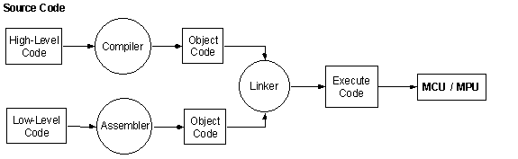
MCU stores only binary numbers, thus instruction set must be in the form of binary numbers. Programming in bin-number is difficult to remember and prone to error (eg, 00100110), this problem can be alleviated using hex-number (eg, 26h). The best approach is to use mnemonic forms (easier to remember) such as ADD, SUB, ...called assembly language (assembly code). Language and Code are interchangeable, code will be used for short. Thus an assembler is required to convert assembly language into machine language (machine code, binary code). Assembly code is much better than a machine code, however it is still difficult to code and is machine-dependent. A programming language similar to our speaking language is thus necessary to facilitate the coding. This language is called high-level language as opposed to low-level language of MCU (machine language). High-level programs are composed of numerous statements, while low-level programs composed of numerous instructions. A statement is equivalent to a couple of instructions, thus a high-level program is shorter than its equivalent low-level program. This is why high-level programming is easier than low-level programming.
Both high-level/low-level programs are called source code. Since computers know low-level code (machine code) only, there must be something to convert a high-level code into low-level code, it is interpreter or compiler. An interpreter executes each statement after each conversion, it is similar to a person interprets each statement of a foreigner for a native. A compiler executes the whole program only after all statements are converted, it is similar a person translate the whole book for publishing to foreign readers. In the past, computers ran so slowly that the executing time is much longer than the reading time, so interpreters were preferred as results could be seen very soon. Nowadays, computers run so fast that the executing time is much shorter than the reading time, thus compilers are preferred. All assembler, interpreter and compiler have another function as debugger to produce error messages.
Some typical codes are:BASIC (Beginners' All-purpose Symbolic Instruction Code: a simple programming language), COBOL (COmmon Business-Oriented Language: a commerce language), FORTRAN (FORmula TRANslation: a scientific calculation language), ALGOL (ALGorithmic Orientd Language), ADA, MODULA, LISP, EIFFEL, FORTH, ...
A huge number of software packages have created to solve many problems in different fields. The disadvantages of low-level coding are time-consuming and prone to errors, but the most serious disadvantage is machine dependence. All low-level programs must be re-coded for a different MCU. All these problems are eliminated using high-level coding, only 1 program has to be recorded, not all, it is the compiler. So high-level programs are called portable, exactly the same C-program can run on PC (C compiler of 80x86) and on UNIX (C compiler of 680x0). The advantages of high-level approach over the low-level are faster coding, shorter source code and hence easier debugging. However, its advantage is its execute time is longer (running slower) and its bigger execute code due to many overheads. These 2 criteria of execute time and code are critical in using MCU for control purpose. Nowadays, MCU is faster and memory is bigger, so high-level code can be used with MCU.
The most popular high-level codes are Basic, Pascal and C since Basic Interpreter is available in MS-DOS software, Pascal and C compilers from Borland (Turbo) and Microsoft are available for PC. Basic is too slow due to its interpreter (up to 50 times slower than C). Assembly code is fastest execute and hardest coding, Pascal is slowest execute and easiest coding, C is in the middle. In addition, C compiler is the smallest , hence the simplest, compiler; it translates a C code text into the assembly code text, then an assembler is used to produce the machine code. Therefore, only C and assembly are used for MCU.
C code
main(void)
{
  int  a, b, c;

  a = 3;
  b = 6;
  if (a < b)
    c = 2;
  else if (a == b)
    c = 5;
  else
    c = 8;
}
Assembly Code
  a  dw  ?			; declaration of variable a, b, c
  b  dw  ?
  c  dw  ?

  mov  a, 3			; a = 3
  mov  b, 6			; b = 6
  mov  ax, a		; ax = a, required for code cmp below
  cmp  ax, b		; compare a, b
  jge  GE
  mov  c, 2			; if a < b
  jmp  END

GE:
  mov  ax, a
  cmp  ax, b
  jne  NE
  mov  c, 5			; if a = b
  jmp  END

NE:
  mov  c, 8			; if a < b

END:
  ret				; stop
Compared to low-level code, high-level code is mush shorter and much easier to understand, since it is similar to our daily-speaking language.
4. MPU/MCU Hardware Interface
4.1. Memory
Memory can be classified into 2 main types: ROM (Read Only Memory), RAM (Random Access Memory). ROM has different versions: OTROM (One Time ROM), EPROM (Erasable Programmable ROM), EEPROM (Electrically Erasable Programmable ROM) and Flashed ROM (cheaper and more reliable than EEPROM). RAM also has different versions: SRAM (Static RAM), DRAM (Dynamic RAM), and Nonvolatile SRAM (SRAM with battery back-up).
Instruction sets are stored in special on-chip ROMs which are unaccessible. Other ROMs are OTROM, EPROM, EEPROM can be used internally or externally, flashed ROM can be used externally only. Information is stored in ROMs by pulses of a ROM programmer, EPROM requires 12.5 V of pulse amplitude, EEPROM requires 5 V amplitude similar to clock pulse. The programming pin of the chip must be asserted in the programming mode so clock pulse cannot corrupt ROMs (EPROM, even EEPROM with 5 V pulse). EPROMs are erased by UV (Ultra Violet) while EEPROM by electrical pulse. MCU has a small on-chip ROM (OTROM, EPROM, EEPROM), if a larger memory is required, an external ROM must be used. The cost of a ROM MCU is much more expensive than that of ROMless MCU plus external larger ROM.
Information is RAM can be erased for storing new information (overwrite), RAM is thus also known as Read-Write Memory, hence data under processing are stored in RAM. On the same chip dimension, hence the same cost, the storage capacity (number of bytes) of DRAM is 4 times that of SRAM. DRAM requires a memory refreshing due the leakage of capacitor (MOSFET) holding information (bit). However, 1 refreshing chip can be used for many DRAM chips, thus DRAM is preferred for a large memory. That is why DRAM of MBs is used in PC (Personal Computer) and SRAM of KBs is used in MCU.
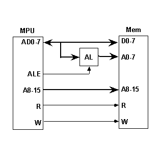
In the real world, to see anybody his/her address must be known. Similarly, to access to any memory location (content) its address must be known. A house-address is a number and its content is a person, while a memory address is also a number but its content is still a number, ie, both are all numbers, it is confusing. The number of address lines determine the memory size.
# @ lines 10 11 12 13 14 15 16 20 SizeNote that
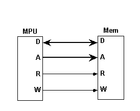
To read or write, MCU sends an address to memory via the address bus, then the signal R or W to the memory via the control bus. Next data are on the data bus, from memory to MCU if R, from MCU to memory if W.
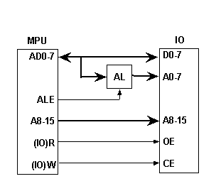
AD0-7 is latched into an address latch by a signal ALE (Address Latch Enable), since these pins AD0-7 will be used for data later.
IP (Instruction Pointer) or PC (Program Counter) is used to store the address of an instruction about to be executed. An execute cycle is composed of
- instruction fetch: MPU fetches instruction which is the content whose address in IP.
- instruction decode: MPU decodes opcode of instruction
- operand fetch: if any of instruction
- instruction execute
IP is automatically increment to the address of the next instruction after each instruction fetch.
4.2. Peripheral Devices (IO Devices)
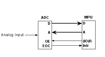
An IO device must have its registers to store data for MPU communicating with the real world. In addition, an IO device must have its address for MPU accessing to. There are 2 approaches of interfacing between MPU and IO device:
- Via a dedicated port if MPU has a spare port and the address of this IO device is that of this port.
- Via the data bus if MPU has no spare port, to recognize data for memory or IO device, there are 2 ways:
- memory-mapped IO: part of an address range is reserved for IO device, if any address in this range, its data must be of IO device, not of memory.
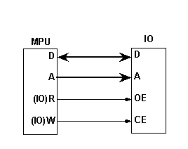
- isolated IO: instruction set has 2 additional special instructions: IN and OUT (software) and control bus has 2 extra special lines: IOR and IOW (hardware) for IO while RD and WR (MR and MW) still for memory; data and address in these 2 instruction are of IO, not memory.
Thus interface between MPU and IO is exactly the same as between MPU and memory if memory-mapped IO is used. Interfacing with an isolated IO is practically the same as with memory, where IN and OUT instructions are used in software, they activate IOR and IOW in hardware, instead of RD (MR) and WR (MW). Normally, MPU uses memory-mapped IO due to its simplicity without IOR/IOW in hardware; while PC uses isolated-mapped IO due to its faster operation with some extra dedicated hardware
Input and output devices have different response speeds, so MPU interfaces with them accordingly.
4.2.1. Output Device
The processing speed of MPU is much faster than that of output devices such as monitor, LCD, printer, ... so output device has its own processor and memory. MPU loads data into memory of output device and continues processing other data. The processor of output device will do the rest (display, print, ...)
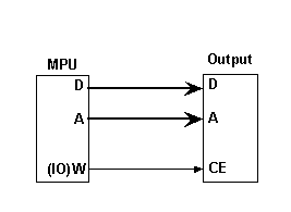
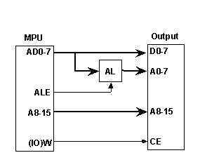
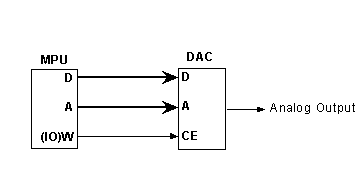
CE (Chip Enable) activates output chip to receive data from MPU.
4.2.2. Input Device
The speeds of input devices are much slower than that of output devices, so far much slower than MPU. Meanwhile, input data are more vital than output data since they are used for processing. For example, in an addition where values x and y are changing and input from keyboard, if input data are missing, MPU will use old values and give wrong result. There are 2 methods to solve this problem: polling and interrupt. In the polling method, MPU does nothing but always polling the input device ready to receive data. But in the interrupt method, MPU keeps doing its own job until interrupted by the input device, the input device send a signal to MPU, MPU finishes its current instruction and receive input data, then returns back to its interrupted job. Therefore, the polling method is simpler as under software control, but not efficient as the interrupt method since MPU has to wait for input data and cannot do anything. However the interrupt method requires an additional line for the interrupt signal in the control bus.
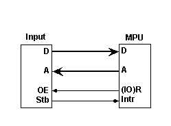
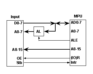
OE (Output Enable) activate an output register to transfer data to MPU via the data bus.
STB (Strobe) informs MPU ready to receive input data.
4.3. Analog Interface
In the real world, all parameters are analog (analog parameter) such as a position of an object on a convey belt, of a drill, .. a temperature in an oven, a height of liquid in a container, ... For these analog parameters under control, they need be converted to electrical signal (analog signal) using a sensor such as thermocouple for temperature. If an analog controller is used, this analog signal is sent directly to the controller composed of numerous op-amps. Nowadays, analog controllers are seldom used since it cannot implement complex control functions and is not flexible. Digital controllers using PC or MCU can implement any control functions regardless complexity. Control function is a text form of control algorithm in a program, so it is extremely flexible. In a digital controller, analog signals must be converted to digital signals by ADC (Analog-to-Digital Converter). When the digital controller completes a control algorithm, the resulted digital signal must be converted to an analog signal for the controlled process to accept. DAC (Digital-to-Analog Converter) is used for this purpose, for example a voltage into a resistor to increase its temperature.
There is an error in conversing between analog and digital signals. For example, a 3-bit digital has only 8 values: 000, 001, 010, ..., 111 equivalent to 0, 1, 2, ...7. Thus, if a 3-bit digital signal is used for a voltage of 0~10 V, we have the mapping below
000	001	010	011	100	101	110	111
0	1	2	3	4	5	6	7
0	 	 	 	 	 	 	10
Then the error is
We can see that the analog signal takes values continuously from 0 to 10, while its digital signal has only 8 discrete values as .
Discretization of an analog signal is characterized by a resolution, for a n-bit ADC/DAC, we have
As n is large enough for , in the example above, has been used for convenience of drawing only, the approximation above cannot be used for this value as with a large error of 0.125. In practice, the minimum value of n is 8, so with tolerance of small enough to be ignored.
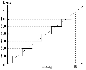
The tolerance can be found from
where
or fullscale, in the above example, span = 10 - 0 = 10.
For example, the resolution of an 8-bit ADC/DAC is with tolerance of 0.02 as span of 10. A 12-bit MCU has a resolution of with tolerance 0.001 with span 10. Thus, ADC/DAC of larger n will be more precise with higher resolution.
4.3.1. Transducer
Normally, a sensor output is too low for noise corruption. An amplifier is required for this signal to have a level high enough to be transferred to MCU via a transmission line, eg, output of a thermocouple is 7~80 mV/0C too low to put on line. For this purpose, we have
Transducer = Sensor + Conditioning IC
where Conditioning IC is a special amplifier.
Transducers are implied analog transducers. Digital transducers have their output in digital signals, so ADCs are not necessary.
There are some MCUs with built-in ADC/DAC such as i80196 from Intel, in these cases the following 2 subsections are out of concerns.
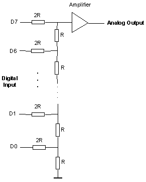
4.3.2. DAC Interface
DAC circuitry is very simple, it requires only some resistors and an op-amp
4.3.3. ADC Interface
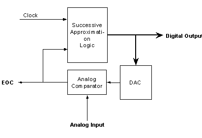
ADC is composed of a digital approximator, DAC and an analog comparator. The digital approximator creates a digital signal for DAC converting to analog signal. The analog comparator then compares this internal analog signal with an external analog input to be converted.
For a span of 5 V analog input, using 8-bit ADC gives
Bit 7	Bit 6	Bit 5	Bit 4	Bit 3	Bit 2	Bit 1	Bit 0
2.5 V	1.25 V	0.625 V	0.3125 V	0.15625 V	0.078125 V	0.0390625 V	0.01953125 V
Note a division by at the subsequent bit: 1000b = 8, 100b = 4, 10b = 2 (b: binary).
The simplest ADC is an architecture whose digital approximator is an up-counter from LSB (bit 0) until the internal analog signal is greater than the external analog signal. For an analog input of , we have
1	10b=2	11b=3	100b=4	. . .	189	190	191
0.01953125	0.0390625	0.05859375	0.078125	. . .	3.69140625	3.7109375	3.73046875
The counter will stop at the count 191 and the digital signal of 3.723 is 191 = BFh.
For an approach of faster conversion but more complex, ADC has a successive approximator starting from MSB (instead of LSB as above) and the analog comparator has to compare only 8 times (instead of 191 times above) where the corresponding bit set 1 if internal analog signal < external analog signal. For the example above with , we have
Step Test Decision Digital Signal
1: 1000,0000(128)	 	Yes	10000000
2: 1100,0000 (192)	 	No	10000000
3: 1010,0000 (160)	 	Yes	10100000
4: 1011,0000 (176)	 	Yes	10110000
5: 1011,1000 (184)	 	Yes	10111000
6: 1011,1100 (188)	 	Yes	1011,1100
7: 1011,1110 (190)	 	Yes	1011,1110
8: 1011,1111 (191)	 	No	1011,1110
The resulted digital signal of analog signal 3.723 is 190 = BEh, thus this result is different from the above by 1, this is the resolution tolerance of any ADC.
Once the analog comparator finishes its job, it sends a signal EOC (End of Conversion) to the digital approximator to stop, and this signal is also sent to MCU as an interrupt signal.
4.3.3. Pulse-Width Modulation (PWM)
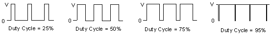
In a 8-bit MCU with PWM, the maximum duty cycle is and the resolution is . If PWM=254, then Vdc=Vcc, PWM=127 gives Vdc=0.5Vcc, PWM=64 yields Vdc=0.25Vcc. Thus, PWM can be used as DAC on its own or with a low-pass filter if necessary.
5. MCU-Based System
5.1. MCU-Based System Architecture
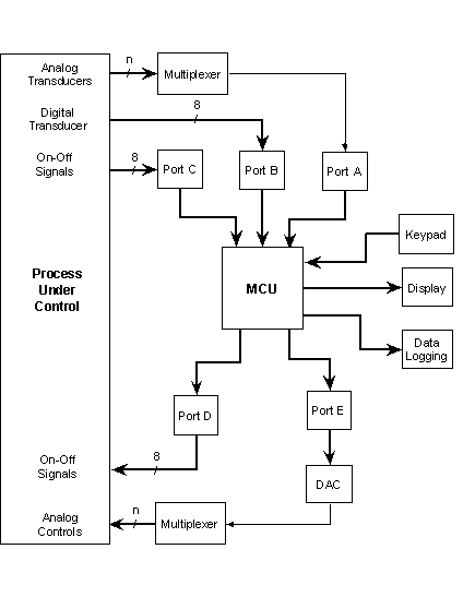
Multiplexer is indeed a multi-position switch
5.2. MCU-Based System Maintenance
The quality of a MCU-based system is determined by that of the program in ROM, 2 systems of exactly the same hardware, one yields better products and higher productivity due to its better program, consequently it is more expensive. For instant, if the hardware cost is $10,000, the system with better program may cost $50,000 while the worse one might cost only $20,000. It is an industry secret and there is usually a protection for ROM such as security pin, self-destroy mechanism, ...Therefore, to maintain a MCU-based system, we should not touch the software (ROM), instead we check hardware only. It is great if we possess a service manual, normally operation manual always available.
In principle, the power supplies should be checked first, then we go from outer to inner, ie, from peripheral devices, IO devices toward MCU. Sensors, transducers and their buffers are deserved great attentions. A buffer is an amplifier between 2 devices, such as between a sensor/transducer and MCU. This part is very crucial as it supplies data for MCU to process. If it is out of order, then there is no data or corrupted data (wrong data), in any case MCU cannot di its job properly. Next are input devices such as ADC, DAC, On-Off signals, keypad, ..., they all are also source of input data for MCU. Then are output devices such as monitor, printer, ... Data logger is used for recording only, generally it does not affect the operation of MCU. However, it is good idea to isolate it from the system.
All digital devices, MCU in particular, are practically very difficult to be out of order. They are working on digital values, logic one of 3.5 ~ 5V, logic zero of 0 ~ 1.5V, they do not require exact values. Most of the cases are due to bad contact, broken connection, wrong voltage supplies (Vcc=5V, Gnd=0V), wrong pulse clock (shape, amplitude, frequency). If external ROM is used, EA (External Access) pin of MCU should be checked for appropriate operation by referring to technical data of that MCU.
5.3. MCU-Based System Implementation
5.3.1. Hardware Implementation
The more powerful MCU (data bits, address bits, number of ports, frequency clock, built-in ADC, ...) is more expensive. The following are some guidelines:
- 8-bit data bus
- 16-bit address bus
- 8 MHz clock
- Built-in ADC (internal ADC), the cost of MCU and ADC chips is often more expensive than that of MCU with internal ADC. If unavailable, using DAC chip under software control for ADC operation is much cheaper (4~5 times) than using ADC, as a trade-off it is slower. For instant, ADC0861 costs $22.50 while $5.50 for DAC0800.
- With or without on-chip ROM, the cost of MCU with on-chip ROM is more expensive than the cost of ROMless MCU and external ROM chips. For example, 87196 MCU with 16 KB on-chip EPROM costs $123.5, while ROMless 80196 MCU is $58.5, and 256KB external EPROM is only $10.5 even higher capacity, only $69 totally, the price. is nearly half of the above.
- The number of ports, similarly to the case of ROMless chip, the cost of MCU with higher number of ports is more expensive than that of chip with lower port number and external IO chip. For example, the cost of 80C552 with 6 ports is $31.50, while the cost of 8031 with 4 ports is $6.00 and 82C55 with 4 ports is $8.00, so $14 for 8 ports compared to $31.50 for only 6 ports.
Nowadays, the most popular families are from Intel and Motorola, if we are familiar with one family, we can easily work with another.
5.3.2. Software Implementation
The very first crucial thing is the memory map of MCU from its technical data (Programming Reference Guide, ...) including the reset address where MCU starts. This map shows us the architecture of MCU, such as data registers (accumulator, ports), control registers, status registers, ADC, PWM, ... with their addresses and some typical application notes (programs). In addition, we need some special equipments such as Development System, EPROM Programmer for checking if desired specifications are achieved before implementation. Development system is rather expensive ($10,000). To promote their products such as 68HC11, i8051, i8096, ..., Intel and Motorola have made Evaluation Boards around $500, they can be used to develop MCU-based systems. Both development system and evaluation board are under PC control.
6. Some Typical Mcu Applications
To control a system, the very first thing is to recognize its inputs and outputs, then identify the system dynamics to obtain a mathematical model of the system. Based on this model, a control function will be determined so that the actual output is equal to the desired output (reference input). This control function (control algorithm) is embedded in an interrupt service routine executed after an equal time interval called sampling time. For simplicity, we will only consider the control algorithm to control position of a DC servo motor, not interrupt routine. To compare a high-level with low-level codes, the programs will be coded in C and assembly of that MCU. Flow chart is a very good tool to present an algorithm (not necessary a control one). The following is a control algorithm to have control a motor for .
6.1. Assembly-Program for MCU 68HC11 from Motorola
For a 68HC11 of 8MHz, we have
        ORG    $0          ;Starting address of RAM
ADVal   equ    $00         ;Up = ADVal
PWMVal  equ    $00         ;Uc = PWMVal

Start                      ;Start of Program
        ORG    $B600       ;Reset address: Starting address of EEPROM
        LDAA   ADVal       ;<3 cycles>
        CMPA   #$82        ;$82: 0+ to eliminate chattering, <2>
        BHI    Hi          ;ADVal > $82 => Up > 0+, <3>
        CMPA   #$7E        ;<2>
        BLO    Lo          ;ADVal < $7E => Up < 0-, <3>
        LDAA   #$80        ; 0- <= Up <= 0+ => Uc = 0 ($80), <2>
        COMA               ;Complement for PWM, <2>
        STAA   PWMVal      ;<3>
        BRA    Exit        ;<3>
Hi      LDAA   #$00        ;If Up > 0+ => Uc = -5V ($00): Negative Feedback, <2>
        COMA               ;Complement for PWM, <2>
        STAA   PWMVal      ;<3>
        BRA    Exit        ;<3>
Lo      LDAA   #$FF        ; If Up < 0- then Uc = +5V ($FF), <2>
        COMA               ;Complement for PWM, <2>
        STAA   PWMVal      ;<3>
Exit
        END                ;End of Program
The hex-code is of 82 bytes in 40 machine cycles (40 x 0.5 = 20 micro-second)
S120B60096008182220B817E250E8680439700200C8600439700200586FF43970041
S9030000FC
6.2. MCS51
For a 80x51 of 12MHz, we have
6.2.1. Assembly-Program ASM51 (fMCU 80752 from Philips)
Start                                    ;Start of Program
      ORG   0         ;Reset address, Always 0
      MOV   R1,#0     ;ADVal, <1> cycle
      MOV   A,#82h    ;X < Y => X-Y < 0 => C=1 => JC: Jump if Carry Set, <1>
      SUBB  A,R1      ;<1>
      JC    Hi        ;82h < R1 => 0+ < Up, <2>
      MOV   A,R1      ;<1>
      SUBB  A,#7Eh    ;<1>
      JC    Lo        ;R1 < 7Eh => Up < 0-, <2>
      MOV   A,#80h    ;0- <= Up <= 0+ => Uc = 0, <1>
      CPL   A         ;Complement for PWM, <1>
      MOV   R2,A      ;PWMVal, <1>
      SJMP  Exit      ;<2>
Hi:   MOV   A,#00h    ;Up > 0+ => Uc = -5, <1>
      CPL   A         ;Complement for PWM, <1>
      MOV   R2,A      ;PWMVal, <1>
      SJMP  Exit      ;<2>
Lo:   MOV   A,#0FFh   ;Up < 0- => Uc = +5, <1>
      CPL   A         ;Complement for PWM, <1>
      MOV   R2,A      ;PWMVal, <1>
Exit:
      END             ;End of Program
This hex-code is of 95 bytes in 22 machine cycles (22 x 1 = 22 micro-second)
:100000007900748299400BE9947E400C7480F4FA74
:0C001000800A7400F4FA800474FFF4FA13
:00000001FF
6.2.2 C-Program: Micro-C
In any code, high or low level, comments are heavily used to show what a statement is doing. Without comments, it is very difficult to know what the program is doing, hence very hard to modify and to maintain. Any program must have comments, as many as possible. These comments will not involve in execute, they serve the user only. In C, comments are between /* and */
/* Use cmnd MC to evoke IDE to compile */

register ADVal=0, PWMVal=0;      /* Up = ADVal, Uc = PWMVal */

main()
{
    if(ADVal > 0x82)          /* Up > 0+ */
        PWMVal = 0;              /* Uc = -V: Negative Feedback */
    else if(ADVal < 0x7E)     /* Up < 0- */
        PWMVal = 0xFF;           /* Uc = +V */
    else                         /* 0- <= Up <= 0+ */
        PWMVal = 0x80;           /* Uc = 0 */
    PWMVal = ~PWMVal;            /* Complement cho PWM for Control Output */
}
As mentioned previously, MCU knows only bin-numbers and its short notation hex-numbers. C compiler translates this C-code (in text) to assembly code (also in text), then it evokes assembler to produce hex-code. The following is an assembly code converted by an c compiler
*
* DDS MICRO-C 8031/51 Startup Code & Runtime library for TINY model
*
* Copyright 1991-1994 Dave Dunfield
* All rights reserved.
*
* System Memory map
        ORG    $0800     ROM Starts here
* Fixed memory locations for alternate access to the CPU register bank.
* If you are NOT useing BANK 0, these equates must be adjusted.
?R0    EQU    0          Used for "POP" from stack
?R1    EQU    ?R0+1      Used to load index indirectly
?R2    EQU    ?R0+2      ""        ""        ""        ""
?R3    EQU    ?R0+3      Used by some runtime lib functions
?R4    EQU    ?R0+4
?R5    EQU    ?R0+5
?R6    EQU    ?R0+6
?R7    EQU    ?R0+7
*
* Startup code entry point
*
* If you are NOT using interrupts, you can reclaim 50 bytes
* of code space by removing the following TWO lines.
    AJMP   *+$0032      Skip interrupt vectors, <2> cycles
    DS     $0032-2      Reserve space for interrupt vectors
*
    MOV    SP,#?stk-1   Set up initial stack, <1>
    LCALL  main         Execute program, <2>
* EXIT to MON51 by calling the 'timer1' interrupt vector.
* This causes MON51 to think that a single-step operation has just
* completed, and therefore it saves the user registers, and performs
* a context switch back to the monitor.
exit        LCALL        $001B                    Call Timer-1 interrupt, <2>
            SJMP        exit                Incase he go's again, <2>
*/* Use cmnd MC to evoke IDE to compile */
*
*register ADVal=0, PWMVal=0;
main EQU *
    MOV    A,ADVal      ;<1> cycle
    OV     B,ADVal+1    ;<1>
    MOV    R3,#130      ;<1>
    MOV    R4,#0        ;<1>
    LCALL  ?gt          ;<2>
    ORL    A,B          ;<1>
    JNZ    *+5          ;<2>
    LJMP   ?AB1         ;<2>
*   PWMVal = 0;
    MOV    A,#0         ;<1>
    MOV    B,#0         ;<1>
    MOV    PWMVal,A     ;<1>
    MOV    PWMVal+1,B   ;<1>
*  else if(ADVal < 0x7E)
    LJMP  ?AB2          ;<2>
?AB1      EQU         *
    MOV   A,ADVal       ;<1>
    MOV   B,ADVal+1     ;<1>
    MOV   R3,#126       ;<1>
    MOV   R4,#0         ;<1>
    LCALL ?lt           ;<2>
    ORL   A,B           ;<1>
    JNZ   *+5           ;<2>
    LJMP  ?AB3          ;<2>
*   PWMVal = 0xFF;
    MOV   A,#255        ;<1>
    MOV   B,#0          ;<1>
    MOV   PWMVal,A      ;<1>
    MOV   PWMVal+1,B    ;<1>
*  else
    LJMP  ?AB4          ;<2>
?AB3      EQU         *
*   PWMVal = 0x80;
    MOV   A,#128        ;<1>
    MOV   B,#0          ;<1>
    MOV   PWMVal,A      ;<1>
    MOV   PWMVal+1,B    ;<1>
?AB4 EQU *
?AB2 EQU *
*  PWMVal = ~PWMVal;
    MOV   A,PWMVal      ;<1>
    MOV   B,PWMVal+1    ;<1>
    LCALL ?com          ;<2>
    MOV   PWMVal,A      ;<1>
    MOV   PWMVal+1,B    ;<1>
*}
    RET                 ;<2>
*
* DDS MICRO-C/51 runtime support functions for ALL memory models
*
* Setup R0 to access the stack
?auto0   XCH    A,R0      Save A, get parameter, <1>
         ADD    A,SP      Adjust for stack offset, <1>
         XCH    A,R0      And restore order, <1>
nargs    RET                            <2>
* Setup R1 to access the stack
?auto1   XCH    A,R1      Save A, get parmater, <1>
         ADD    A,SP      Adjust for stack offset, <1>
         XCH    A,R1      And restore order, <1>
         MOV    R2,#0     Clear high of index, <1>
         RET              <2>
* Adjust the stack pointer by R7 bytes
?adjstk  OP    DPH        Get high byte of RET addr, <2>
         POP   DPL        Get low byte of RET addr, <2>
         XCH   A,R7       Get adjust (and save A), <1>
         ADD   A,SP       Adjust stack, <1>
         MOV   SP,A       Set new value, <1>
         XCH   A,R7       Restore A (& return new stack), <1>
         PUSH  DPL        Resave low, <2>
         PUSH  DPH        Resave high, <2>
         RET                           <2>
* Clean up stack & exit function
?exit     XCH  A,R7       Get adjust (save A), <1>
         ADD   A,SP       Adjust stack, <1>
         MOV   SP,A       Resave, <1>
         XCH   A,R7       Restore A (& return new stack), <1>
         RET              <2>
* One's complement the 16 bit accumulator
?com     CPL   A          Complement low byte, <1>
         XCH   A,B        Swap it, <1>
         CPL   A          Complement high byte, <1>
         XCH   A,B        Reorder, <1>
         RET              <2>
* Signed compares
?lt      LCALL ?scomp     AB < R3-4 (signed), <2>
         JC    ?ret1      <2>
         SJMP  ?ret0      <2>
?le      LCALL ?scomp     AB <= R3-4 (signed), <2>
         JC    ?ret1      <2>
         JNZ   ?ret0      <2>
         SJMP  ?ret1      <2>
?gt      LCALL ?scomp     AB > R3-4 (signed), <2>
         JC    ?ret0      <2>
         JNZ   ?ret1      <2>
         SJMP  ?ret0      <2>
?ge      LCALL ?scomp     AB >= R3-4 (signed), <2>
         JNC   ?ret1      <2>
         SJMP  ?ret0      <2>
* Equality compares
?eq      LCALL ?ucomp     AB == R3-4, <2>
?eq1     JZ    ?ret1      They are the same, <2>
?ret0    CLR   A          Get zero, <1>
         MOV   B,A        Set high, <1>
         RET              Return logical ZERO, <2>
?ne      LCALL ?ucomp     AB != R3-4, <2>
         JZ    ?ret0      <2>
?ret1    CLR   A          Get zero, <1>
         MOV   B,A        Set high, <1>
         INC   A          Convert to 1, <1>
         RET              Return logical ONE, <2>
* Signed ompare of AB & R3-4
?scomp   CLR   C          Clear borrow, <1>
         SUBB  A,R3       Calculate difference (low), <1>
         XCH   A,B        Get high, <1>
         SUBB  A,R4       Calculate difference (high), <1>
         JB    A.7,?sco2  Negative == <, <2>
         JB    PSW.2,?sco3    Overflow == <, <2>
?sco1    CLR   C          Indicate not less than, <1>
         ORL   A,B        Setup 'Z' if equal, <1>
         RET              <2>
?sco2    JB    PSW.2,?sco1    Negative & overflow == !<, <2>
?sco3    SETB  C              Indicate less than, <1>
         RET                  <2>
* Unsigned compare of AB & R3-4
?ucomp   XCH   A,B       Get high, <1>
         CLR   C         Zero high, <1>
         SUBB  A,R4      Compare high, <1>
         JNZ   *+5       Different, <2>
         MOV   A,B       Get low, <1>
         SUBB  A,R3      Compare low, <1>
?ucomp1  RET             <2>
* S/N: 1337
*
* DDS MICRO-C/51 runtime library support files for TINY models
*
* Load a byte from external memory into TEMP register
?extb    MOV   R3,A          Save A, <1>
         CLR   A             Zero offset, <1>
         MOVC  A,[A+DPTR]    Get the byte, <2>
         XCH   A,R3          Restore A, save result, <1>
         RET                 <2>
* Load a word of external memory into TEMP register
?extw    MOV   R4,A          Save A, <1>
         CLR   A             Zero offset, <1>
         MOVC  A,[A+DPTR]    Get the low order byte, <2>
         MOV   R3,A          Save result LOW, <1>
         MOV   A,#1          Offset to HIGH, <1>
         MOVC  A,[A+DPTR]    Get the high order byte, <2>
         XCH   A,R4          Restore A, save result HIGH, <1>
         RET                 <2>
* Load a word of external memory into INDEX register
?exti    MOV   R2,A          Save A, <1>
         CLR   A              Zero offset, <1>
         MOVC  A,[A+DPTR]    Get the low order byte, <2>
         MOV   R1,A          Save result LOW, <1>
         MOV   A,#1          Offset to HIGH, <1>
         MOVC  A,[A+DPTR]    Get the high order byte, <2>
         XCH   A,R2          Restore A, Save result HIGH, <1>
         RET                 <2>
*#map1 Segment 1, initialized variables
ADVal    DRW 0
PWMVal   DRW 0
*
*main()
*{
*  if(ADVal > 0x82)
*#map2 Segment 2, internal "register" variables
         ORG    $0008       Internal ram ALWAYS starts here
* S/N: 1337
* Define the stack (at the end of segment 2)
?stk     EQU    *           Stack goes at top of user variables
* S/N: 1337
*
* Suffix file, define heap memory at the end of all pre-allocated storage.
*
?heap    EQU    *          End of allocated memory
* S/N: 1337
The sequel is the hex-code of 630 bytes running in 192 machine cycles (192 x 1 = 192 mircro-second)
:020800000132C3
:2008320075810712083D12001B80FBE5268527F07B827C001208CE45F0700302085D74001F
:2008520075F000F52885F029020887E5268527F07B7E7C001208BE45F0700302087D74FF3F
:2008720075F000F52885F029020887748075F000F52885F029E5288529F01208B7F5288583
:20089200F02922C82581C822C92581C97A0022D083D082CF2581F581CFC082C08322CF25E5
:2008B20081F581CF22F4C5F0F4C5F0221208F14029801E1208F140227017801E1208F140DB
:2008D200107017800C1208F1501080051209056009E4F5F02212090560F7E4F5F00422C356
:2008F2009BC5F09C20E70720D207C345F02220D2F9D322C5F0C39C7003E5F09B22FBE4936E
:18091200CB22FCE493FB740193CC22FAE493F9740193CA22000000001E
:00000001FF
6.3. Intel MCS96 Family
1 State = 2 Clock
For a 80C196KB12, we have
6.3.1. Assembly Program ASM96
$DEBUG ERRORPRINT NOSYMBOLS
;****************************************************************************
;  CTL_A96.A96 - Cmd "96al ctl_a96" to assemble and link
;****************************************************************************
CTL MODULE   MAIN,STACKSIZE(20)
$NOLIST INCLUDE (80C196KB.INC)
$LIST

RSEG  AT 30h
    RSV:  DSW   8           ; Reserve space in RISM

RSEG
    ADVal        equ    00h
    PWMVal    equ    00h

CSEG  AT 2080h
INIT:
    CMPB    ADVal,#82h      ;$82: 0+ to eliminate chattering, <5>
    JH      Hi              ;ADVal > $82 => Vp > 0+, <4|8>
    CMPB    ADVal,#7Eh      ;<5>
    JNH    Lo               ;ADVal < $7E => Vp < 0-, <4|8>
    LDB    R0,#80h          ; 0- <= Vp <= 0+ => Vc = 0 ($80), <5>
    NOTB    R0              ;Complement for PWM, <3>
    LDB    PWMVal,R0        ;<4>
    BR    Exit              ;<7>
Hi:
    LDB     R0,#00h         ; If Vp > 0+ then Vc = -5V ($00): Negative Feedback, <5>
    NOTB    R0              ;Complement for PWM, <3>
    LDB    PWMVal,R0        ;<4>
    BR    Exit
Lo:
    LDB    R0,#0FFh         ; If Vp < 0- then Vc = +5V ($FF), <5>
    NOTB    R0              ;Complement for PWM, <3>
    LDB    PWMVal,R0        ;<4>
Exit:
    END
The sequel is the hex-code of 128 bytes running in 61 state timess (61 x 0.167 = 10.167 mircro-second)
:10208000998200D90F997E00D114B180001200B05E
:1020900000002012B100001200B000002008B1FFC3
:0620A000001200B0000078
:00000001FF
6.3.2. C-Program: iC96
/* Cmd "96cl ctl_a96" to compile and link */

#pragma  model(kb)	/* Select instruction set for the 80C196KB uP   */

#include <80c196.h>  /* Include header file that declares variables to access
		      * AD channel, HSO, SW_Timer0, Interrupr Flag (IF),
		      * and also enable() to enable global interrupt       */


main()
{
    register unsigned char ADVal=0, PWMVal=0;
    if(ADVal > 0x82)
        PWMVal = 0;
    else if(ADVal < 0x7E)
        PWMVal = 0xFF;
    else
        PWMVal = 0x80;
    PWMVal = ~PWMVal;
}
The following is an assembly program (ctl_c96.lst) created by iC96
iC-96  Compiler   CTL_C96                                                                    11/01/96 15:42:55  Page   1


DOS 6.20 (046-N) iC-96 Compiler X234, Compilation of module CTL_C96
Object module placed in ctl_c96.obj
Compiler invoked by: d:\mcs\mcs96\ic96\bin\IC96.EXE ctl_c96.c96 debug code

 Line Level  Incl

  1    /* Use cmnd MC to evoke IDE to compile */
  2
  3    #pragma  model(kb)   /* Select instruction set for the 80C196KB uP      */
  4
  5    #include <80c196.h>  /* Include header file that declares variables to access
  6                             * AD channel, HSO, SW_Timer0, Interrupr Flag (IF),
  7                             * and also enable() to enable global interrupt    */
  8
  9
 10       main()
 11       {
 12   1       register unsigned char ADVal=0, PWMVal=0;
 13   1       if(ADVal > 0x82)
 14   1           PWMVal = 0;
 15   1       else if(ADVal < 0x7E)
 16   1           PWMVal = 0xFF;
 17   1       else
 18   1           PWMVal = 0x80;
 19   1       PWMVal = ~PWMVal;
 20   1   }

            Assembly Listing of Object Code

                                           ;   Statement    11
        0000              main:
        0000  C800     R     push  ?OVRBASE      ;<6>
                             ;   Statement    12
        0002  1100     R     clrb  ADVal         ;<3>
        0004  1101     R     clrb  PWMVal        ;<3>
                             ;   Statement    13
        0006  998200   R     cmpb  ADVal,#82H    ;<5>
        0009  D104           bnh   @0002         ;<4|8>
                             ;   Statement    14
        000B  1101     R     clrb  PWMVal        ;<3>
                             ;   Statement    15
        000D  200D           br    @0003         ;<7>
        000F              @0002:
        000F  997E00   R     cmpb  ADVal,#7EH    ;<5>
        0012  DB05           bc    @0004         ;<4|8>
                             ;   Statement    16
        0014  B1FF01   R     ldb   PWMVal,#0FFH  ;<5>
                             ;   Statement    17
        0017  2003           br    @0005         ;<7>
        0019              @0004:
                              ;   Statement    18
        0019  B18001   R      ldb   PWMVal,#80H  ;<5>
        001C              @0005:
        001C              @0003:
                             ;   Statement    19
        001C  AC011C   R     ldbze Tmp0,PWMVal   ;<4>
        001F  021C           not   Tmp0          ;<3>
        0021  B01C01   R     ldb   PWMVal,Tmp0   ;<5>
                             ;   Statement    20
        0024  CC00     R     pop   ?OVRBASE      ;<11>
        0026  F0             ret                 ;<11>

                             end
The sequel is the hex-code of 176 bytes running in 91 state timess (61 x 0.167 = 15.167 mircro-second)
:10208300C81A111A111B99821AD104111B200D9918
:102093007E1ADB05B1FF1B2003B1801BAC1B1C02A6
:0720A3001CB01C1BCC1AF05D
:03208000E727004F
:0720AA00A12A0018EFD2FF8C
:00000001FF
6.4. Discussion
    Hex Code(bytes)    MachineCycles    Execute Time(Micro-Second)
Assembly 68HC11 (Motorola) - 8 MHz    82    40    20
Assembly MCS51 (Intel) - 12 MHz    95    22    22
Micro-C Language    630    192    192
Assembly MCS96 (Intel) - 12 MHz    128    61    10
iC96 Language    176    91    15
We have seen that a C-program is very similar to our daily language, iC96 has resulted a resonable hex-code, however Micro-C hex-code is so big by a very large overhead due the very inefficient C-compiler (Dave Dunfield), this certainly slow down the execute. This hex-code cannot be loaded into a 68HC11 as this MCU has only 512 bytes. Compared with Motorola, the hex-code by assembly Intel is a little bigger, but faster 2 times.
6.5. Assembly Intel / Motorola
*    8051 (Intel) has both binary and unary operators, while 68HC11 (Motorola) has only unary operator
    * 68HC11:
                LDAA   #10             ;A <- 10
                STAA   Data            ;Data <- A (10)
    * 8051:     Operator    Dst,Src    ;Destination, Source
                MOV    Data,#10        ;Data <- 10

*    68HC11 and MCS96 have Conditional Branch, but MCS51 has none
    * 68HC11 :
                LDAA   #0
                CMPA   Data
                BLO    Lo              ;Go to Lo if 0 < Data
    * 8051: smaller - larger will set carry bit (carry bit = 1)
                MOV    A,Data
                SUBB   A,#0            ;Data - A(0)
                JC     Lo              ;Data < 0 => Data - 0 < 0 => Carry = 1 => Jump Carry if Set
*    68HC11 has reset address at B600h of on-chip EPROM, while 8051 @ 0h, and 80C196 @2080h